Xunhomon

EMC Basics

1. What's EMC, EMI, EMS

EMC (Electromagnetic Compatibility) :

refers to the ability of electronic or electrical devices or systems to operate within their intended electromagnetic environment without suffering from degraded performance, loss of functionality, or damage caused by the surrounding electromagnetic environment, nor to produce excessive electromagnetic energy that can interfere with the normal operation of surrounding equipment.

EMI (Electromagnetic Interference) :

refers to the limit on self-generated electromagnetic interference.

EMS (Electromagnetic Susceptibility) :

refers to the range of self-supplied electromagnetic interference.

The electromagnetic environment varies with the environment in which the same type of product is used, and thus different standards apply.

It should be noted that all of the above are based on the premise that devices or systems are operating normally in a certain environment.

2. EMI

1) The cause of electromagnetic interference is the unnecessary part of the voltage/current variation.

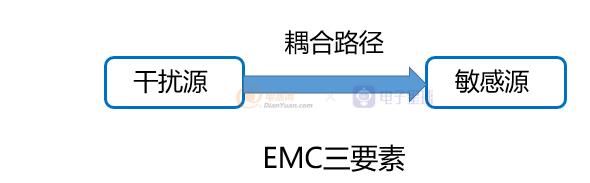
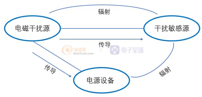
2)There are two coupling pathways for electromagnetic interference:

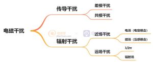
Conducted via wires and radiated through space.

The reason for conducted interference is that current always flows through the “minimum impedance” path.

Taking shielding wires as an example:

at low frequencies (f<1kHz), the wire resistance plays a major role, and most of the current flows through the copper wire of the conductor; 

at high frequencies (f>10kHz), the inductive impedance of the shielding layer is less than the impedance of the wire, so the signal current flows through the shielding layer.

3) Interfering currents propagate through wires in two ways: common mode and differential mode.

The useful signal is generally a differential signal, so common-mode current can only interfere with the useful signal after being transformed into differential-mode current. Impedance balance prevents the common-mode current from converting to differential mode. Multi-point grounding can be used to reduce ground impedance, thereby reducing common-mode ground impedance interference.

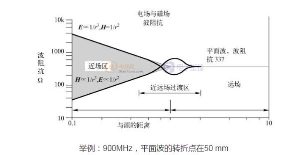
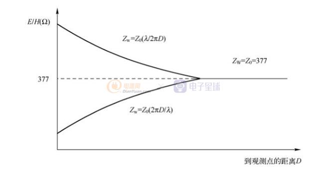
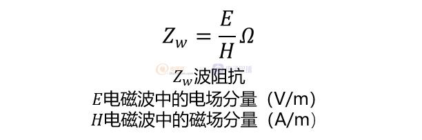
4) Radiated interference is divided into near field and far field.

The near field is also called the induction field, which is closely related to the properties of the field source.

When the source is high voltage and low current, it mainly manifests as an electric field;

When the source is low voltage and high current, it mainly manifests as a magnetic field.

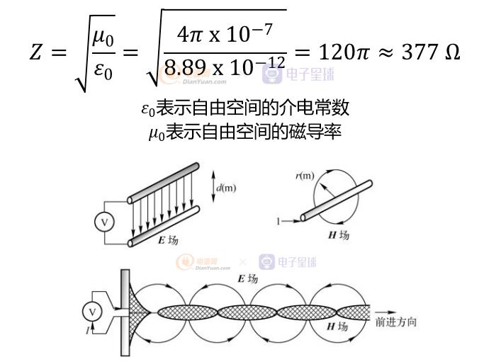
Whether it is an electric field or a magnetic field, when the distance is greater than λ/2π, it becomes a far field.

The far field is also called the radiation field. The far field belongs to plane waves, which are easy to analyze and measure, while the near field has the problem of mutual conversion between electric fields and magnetic fields, which is more complicated.

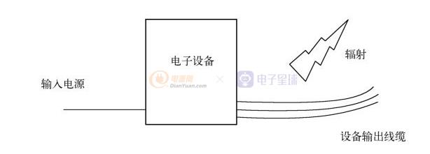
The problem is, what if the wires become antennas? Sometimes it is difficult to distinguish between conducted interference and radiated interference.

In the low-frequency band, especially below 30 MHz, conducted interference is the main issue. Alternatively, it can be estimated that when the length of the equipment and wires is shorter than the wavelength, the main problem is conducted interference, and when their size is longer than the wavelength, the main problem is radiated interference.

The interference signal is radiated as electromagnetic field energy in the form of a plane electromagnetic wave, and then enters the interfered lines, equipment, or systems through leakage and coupling in the form of insulation supports (including air) as a medium, via common impedance coupling.

5) Electric wave radiation requires two necessary conditions: 

changing voltage/current and a radiating antenna. 

Without either, significant radiation interference will not be generated.

Some materials may provide the concept of transient interference, which is electromagnetic interference with short duration but high amplitude, as the name suggests.

Transient interference generally refers to three types of electrical fast transient (EFT), various surges (SURGE), and electrostatic discharge (ESD).

3. EMC three elements

1) Emission control

2) Immunity control

3) Grounding and bonding


Key point: Eliminating any one of these elements can meet the requirements of electromagnetic compatibility design.

Cutting off the coupling path is the most effective measure for electromagnetic compatibility processing.

It is important to understand the propagation path:

Electromagnetic interference can be propagated through conductive interference pathways such as power lines, signal lines, ground lines, and earth, as well as through direct space propagation as radiated interference.

These interferences or noise do not exist independently, and new complex noise may appear during propagation. The problem of these overlapping issues is the difficulty in solving the problem

4.

In the near-field zone, the wave impedance is related to the position, impedance, frequency, and surrounding medium of the radiation source; 

In the far-field zone, the wave impedance is equal to the characteristic impedance of the electromagnetic wave propagation medium. In a vacuum, the wave impedance is 377 Ω.

The 377 Ω characteristic impedance of free space can be derived from this value.

There is a basic concept that needs to be explained: the difference between dB and dBm. 

dB is a commonly used term. dBm is the value of power relative to 1 mW.

As for the difference, it can be expressed directly by the formula:

5. Loop

One reason for PCB radiation emissions is the loop formed by the current in the transmission path and the return path.

In electronic products, there is a loop in the transmission of any signal. If the signal is alternating, the loop will produce radiation. After the current size and frequency of the signal in the product are determined, the radiation intensity produced by the signal loop is related to the loop area. Controlling the area of the signal loop can control EMC issues.

5.1 Single-point grounding & multi-point grounding

The choice of whether to use single-point grounding for electronic devices mainly depends on the frequency of the system’s operating signal and the length of the ground wire, characterized by the parameter L/λ.

When L/λ <= 0.1, single-point grounding is preferred, and the application range of single-point grounding is generally below 300 kHz, and in some cases, it can also be used below 1 MHz.

When the length of the ground wire is an odd multiple of 1/4 wavelength, the ground wire impedance becomes very high, causing antenna effects, where the ground wire radiates noise signals like an antenna.

If a single-point grounding is used, the length of the ground wire should not exceed 1/20 of the wavelength; otherwise, a multi-point grounding should be used.

5.2 Heat dissipation & Shielding

Shielding and heat dissipation are contradictory to each other. 

Heat dissipation holes are usually a group of holes that use forced convection by a fan. These holes will cause electromagnetic leakage, reducing the shielding effect. The larger the holes, the worse the shielding effect.

Usually, the system’s housing is equipped with heat dissipation holes, which will affect the shielding performance of the entire system.

6. EMC Test

Electromagnetic compatibility testing is divided into two categories:

One is Electromagnetic Interference (EMI) testing, which tests the emission characteristics of electronic product systems for interfering with other devices and the electromagnetic environment.

The other is Electromagnetic Susceptibility (EMS) testing, which tests the ability of electronic devices to resist spatial electromagnetic interference.

The national standard has two EMI testing items, while the military standard has seven. 

The EMS testing items are 10 for the national standard and 12 for the military.

And this difference in testing items reflects different requirements for different industries.

EMC testing has different standards, and different industries must follow their own standards to determine the level and requirements they need to meet.

6.1 EMI Testing Items

1. Conducted Emissions (CE) testing (power line, signal, control line)

2. Radiated Emissions (RE) testing

3. Harmonic measurement

4. Voltage fluctuation and flicker measurement

There are three types of EMI testing sites: semi-anechoic chamber, fully anechoic chamber, and open area test site.

6.2 EMS Testing Items:

1. Electrostatic Discharge Susceptibility (ESD)

2. Electrical Fast Transient/Burst Susceptibility (EFT)

3. Surge Testing

4. Radiated Susceptibility (RS)

5. Conducted Susceptibility (CS)

6. Voltage Dips and Interruptions (DIP)

6.4 The advised direction when EMC test fail

Product-related EMC testing is essential. If there are issues detected during the testing, here are some corrective actions that can be taken:

1. Electrostatic discharge susceptibility testing –> Shielding

2. Electrical fast transient/burst susceptibility testing –> Power isolation, use of shielded twisted pair wire & installation of magnetic rings.

3. Surge testing –> Installation of surge suppressors

4. Conducted susceptibility due to radiofrequency (RF) field induction –> Shielding, grounding, and filtering

5. Radiated susceptibility due to RF electromagnetic field radiation –> Pressing cables with conductive foam to minimize gaps

6. Conducted emissions –> Power isolation, filtering, grounding, and reducing the loop area.

7. If there is an exceedance of radiation emission standards –> Shielding and grounding, checking connections, installing magnetic rings, and inspecting simulated devices.

7. Summary

To design the electromagnetic compatibility of a product, every step must be considered from overall design, including circuit design, component selection, PCB production, prototype debugging, testing, and release. Electromagnetic compatibility issues need to be taken into account at every stage, from initial planning to final certification, to successfully control electromagnetic compatibility problems. Only with the concept of electromagnetic compatibility design incorporated in every design step can these issues be genuinely controlled.

If you think it’s helpful, welcome to share to your SNS network.

We're ready to help you grow profit with Bamboo charging products in the coming months, don't hesitate to contact us Today!