Apple introduced wireless charging technology to iPhones starting from the iPhone 12, igniting the entire industry. As ordinary consumers, in addition to using wireless charging every day, we are curious about how wireless chargers are manufactured. Now let’s take a closer look at the production process of a wireless charger.
A typical wireless charger consists of two main parts: the internal circuit board and the external casing. In this production process, we will provide a detailed introduction from these two aspects.
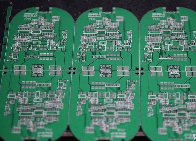
The image above shows an empty board without any electronic components. It is first placed on a fully automatic solder paste printer to apply a layer of solder paste. The solder paste is a mixture of solder powder, flux, and other surface-active agents and thickeners. As seen in the image, this wireless charger circuit board has more than 30 components.
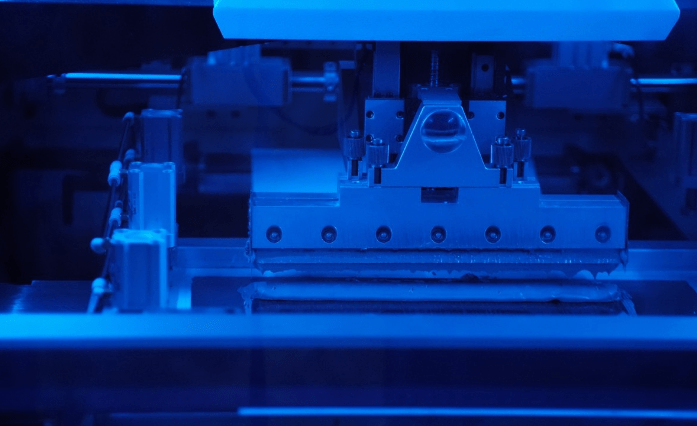
The image above shows a fully automatic solder paste printer. The next step is Surface Mount Technology (SMT) placement. SMT, short for Surface Mount Technology, is widely used in the electronics industry and is mainly used for the installation of electronic components without pins or with short pins.
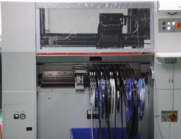
The SMT placement machine sequentially installs and secures chips, resistors, capacitors, inductors, and other components onto the circuit board with solder paste applied.
Each SMT high-speed placement machine is controlled by a small computer, and engineers design the material usage and program the preset operating procedures for each wireless charger circuit board, greatly improving the placement accuracy of the circuit board.
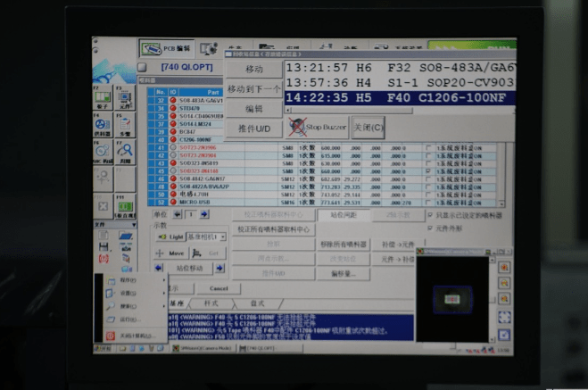
Electronic components are installed in specific positions and order, as shown in the lower right corner of the image, where a chip is being installed.
The assembled circuit board goes through reflow soldering. Reflow soldering involves blowing heated air or nitrogen gas onto the assembled board to connect the circuit. The image above shows the reflow soldering operation using lead-free environmentally friendly processes. The equipment on the right is the reflow soldering machine, with an internal temperature reaching over 200 degrees Celsius.
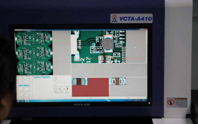
After solder paste application, SMT placement, and reflow soldering, the PCB board has transformed into a complete PCBA. At this stage, the PCBA needs to be inspected to ensure the proper functioning of each part. The image above shows the inspection of the PCBA using an automated optical inspection (AOI) machine. With magnification, it is possible to visually check for issues such as solder voids and missing solder during the chip and component placement process.
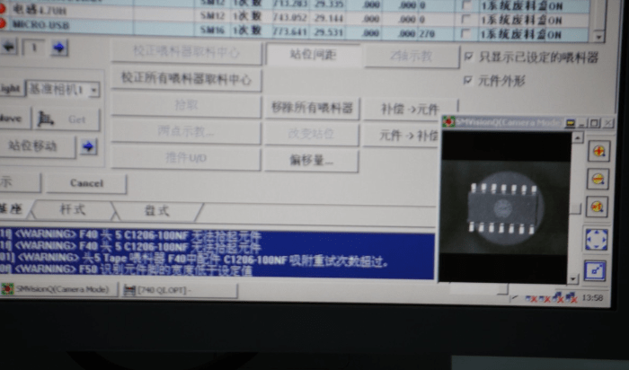
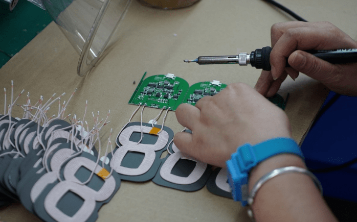
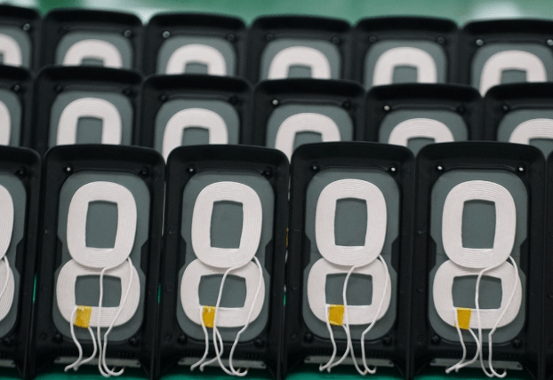
Once the PCBA passes the inspection, it proceeds to the next process: welding the transmission coils.
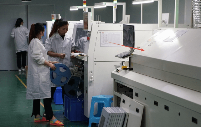
The welding of the transmission coils requires manual operation. As seen in the image, the technician’s left hand wears a blue wristband with a grounding wire to prevent electrostatic discharge from damaging the high-precision chips.
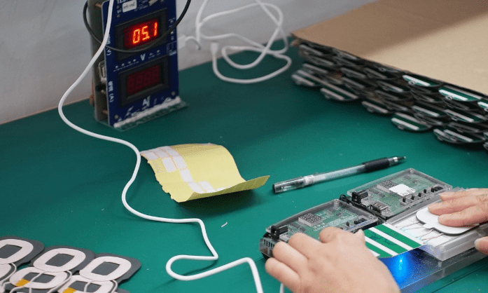
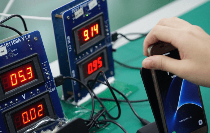
Next, the functionality of the transmission coil board is tested to ensure it operates correctly under different input voltages.
The image above shows the voltage and current during fast charging of the wireless charger, which is 9V/1.7A
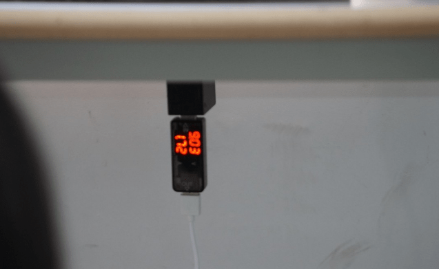
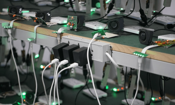
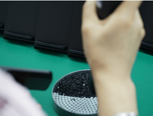
This process is the aging test. Each qualified wireless charger undergoes power-on, load, and other tests before leaving the factory. This helps identify any defective products during the testing process. Wireless chargers with successful aging tests proceed to the assembly stage, while defective ones are isolated for troubleshooting. According to engineers at the factory, the aging test for a single-coil wireless charger takes approximately 2 hours, while a dual-coil charger takes around 4 hours.
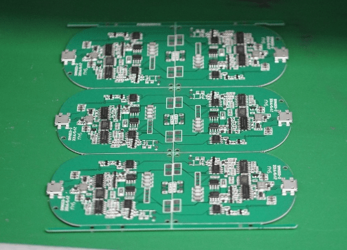
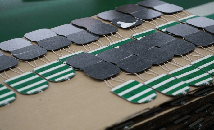
The image above shows the PCBs of the wireless chargers after the aging test, neatly arranged. The electronic components are facing downward to avoid any damage during handling.
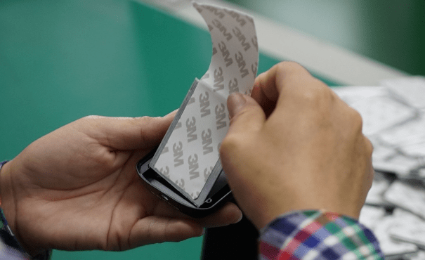
The transmission module is secured to the wireless charger casing using 3M adhesive.
The image above shows the semi-finished wireless charger with the transmission module already assembled, waiting for the next assembly process.
Screws are tightened.
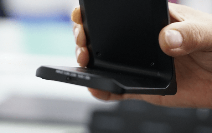
A vertically standing wireless charger with dual-coil fast charging is now assembled.
A real device test is conducted before leaving the factory. As seen in the image, a Samsung wireless charging phone is being used. This step is carried out to ensure the compatibility of the wireless charger and to guarantee that the wireless charger delivered to users provides an equivalent performance experience to the original charger.
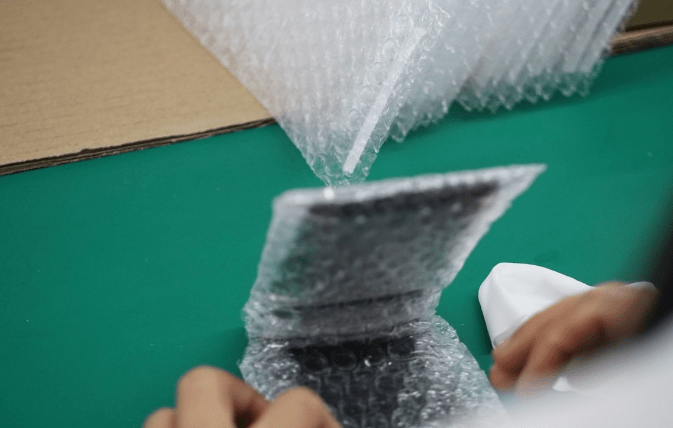
The wireless charger is protected using bubble wrap to ensure its safety during transportation.
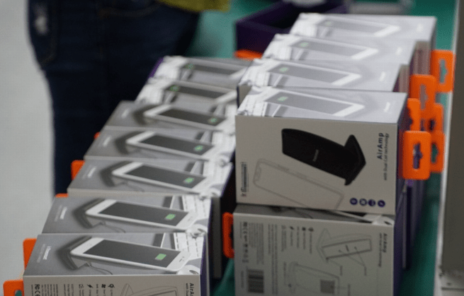
It is then packaged in a box and circulated worldwide.
The above is the complete production process of a wireless charger, which can be summarized as follows: empty board printing, SMT placement, reflow soldering, PCBA inspection, coil welding, testing, aging test, adhesive application, casing assembly, finished product testing, and packaging. After reading this, do you have a detailed understanding of the mysterious production process of wireless chargers?
If you think it’s helpful, welcome to share to your SNS network.