Xunhomon

Solution to EMC problems

All of our wireless charging stations need to pass CE, RoHS, FCC, then engineers need to solve EMC problems in order to meet the requirements. 

Regardless of the electronic product, EMC is always a problem that needs to be faced. 

EMC stands for Electromagnetic Compatibility and is divided into two parts: EMS (electromagnetic susceptibility) and EMI (electromagnetic interference), which evaluate the product’s own stability and external noise level, respectively. 

These are important indicators of product quality. Tthis article introduces the basic principles of EMC and electrostatic surge, as well as common solutions, which can guide engineers in PCB layout and solving practical EMC problems.

Everything in the world has interference. Only with interference can there be anti-interference. 

There are three major directions for solving EMC problems, and around these three directions, many solutions can be derived. These three major directions are interference sources, interference propagation paths, and interference receivers.

In terms of interference propagation paths, there are two types: spatial and conduction, and different paths have different interference sources.

Let’s start with spatial interference. 

The following figure is a schematic diagram of the three classifications of spatial interference: electrostatic coupling, electromagnetic coupling, and radio wave electromagnetic coupling. 

The noise generated by the interference source affects the receiving circuit through these three spatial paths, which can cause system abnormalities.

1. Electrostatic coupling

Electrostatic coupling is sensitive to the electric field and generally has high voltage and low current. 

Its simplified model is as follows: there is capacitive coupling between the interference source and the victim, the electric field generated by the interference source will act on the victim through the capacitor (on the order of pF), which can cause noise in the victim, which is electrostatic interference.

If the victim has high impedance, the generated interference will also be amplified. This is one of the reasons why high-impedance circuits are more susceptible to noise.”

What are the methods to mitigate the interference caused by electrostatic coupling?

1) Increase spacing

Reduce the coupling capacitance to reduce interference.

2) Shorten the coupling length

Reduce the length of the parallel portion of the two traces, which can reduce the parallel capacitance and thus reduce the interference caused by coupling capacitance.

3) Electrostatic shielding

Metal grounding shielding can block the interference source and the victim, as shown in the figure.

4) Reduce the voltage of the interference source

5) Add filters to the source end of the interference source

2. Magnetic coupling

With love comes hate, and with capacitance comes inductance. 

The two are dual devices, and electromagnetic coupling is based on inductive coupling with low voltage and high current. When a current flows through a wire, it generates a magnetic field, which can affect adjacent circuits through mutual inductance, causing interference. This is magnetic coupling.

So what are the methods to mitigate the interference caused by electromagnetic coupling?

1) Increase spacing

Reduce the mutual inductance to reduce interference.

2)Shorten the coupling length and use perpendicular crossing traces

Reduce the length of the parallel portion of the two traces, which reduces the mutual inductance.

3)Electromagnetic shielding

Through a metal plate eddy current to block the magnetic field, which can be ungrounded. If the metal plate is used for return current, it should be grounded.

4)Reduce the current of the interference source

5)Add filters to the source end of the interference source

3. Electromagnetic coupling and antennas

Electrostatic coupling and magnetic coupling are sensitive to distance, which is near-field interference. Increasing distance can greatly reduce interference. 

However, interference from radio waves is far-field interference and not very sensitive to distance.

Antennas can generate radio waves and can be divided into dipole antennas and loop antennas, as shown in the figure. These antennas can both transmit signals and receive signals (pick up noise). 

Therefore, when used as transmitting antennas, we should try to avoid interference generated by the antennas; for victim devices, we should try to avoid the internal design of useless antennas, which can pick up radio wave interference.

Dipole antennas are sensitive to voltage, and loop antennas are sensitive to current.

4. Dipole antennas

For a dipole antenna, it is more likely to generate radio waves when its length is half the wavelength.

For example, for a 750MHz signal, its speed after being transmitted into the air is the speed of light 3*10^8 m/s, and the wavelength is 400mm, so half of the wavelength is 200mm. 

Therefore, if the antenna length is less than 200mm, it can help reduce interference.

λ=C/f, λ: wavelength, C: speed, f: frequency

Adding an LC filter in front of the antenna can suppress high-frequency harmonics to reduce EMI and achieve impedance matching for optimal transmit power

When routing, we should also avoid individual wire ends as it may act as transmitting or receiving antennas, picking up radio wave interference.

5. Loop antennas

Many magnetic field detection devices based on Faraday’s law of electromagnetic induction use probe coils to pick up magnetic fields. 

Loop antennas can both transmit and receive radio waves, and reducing the area of the transmitting loop antenna is one effective way of reducing interference. 

When doing PCB layout, we should also shorten the length of the routing to avoid forming transmitting or receiving loop antennas.”

6. Near field and far field

Near field and far field are a very important pair of concepts that play an important role in guiding us to optimize EMC.

The boundary between the near field and the far field is d=λ/2π, where λ is the wavelength. When the distance between the antenna is less than d, it is near field, and when it is greater than d, it is far field.

Dipole antennas have a stronger electric field in the near-field region and the electric field decays faster with distance.

Loop antennas have a stronger magnetic field in the near-field region and the magnetic field decays faster with distance.

However, whether it is a dipole antenna or a loop antenna, in the far-field region, the electric and magnetic fields decay at the same rate with distance, and the wave impedance at this time is 377Ω, which is an important parameter that will be used later.

7.Suppression of conducted noise

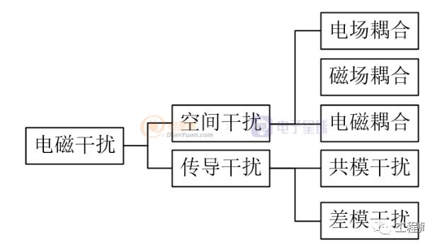
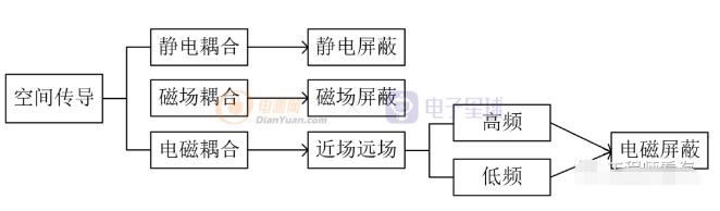
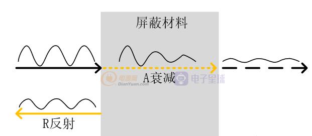
The methods for suppressing noise caused by electrostatic and electromagnetic coupling have been discussed earlier and will not be repeated here. This section introduces the suppression of electromagnetic interference by shielding materials, which is also called electromagnetic shielding.

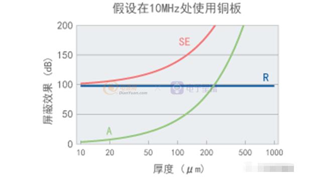
The shielding effect can be approximately expressed as SE = R + A, where R represents the reflection loss and A represents the attenuation loss.

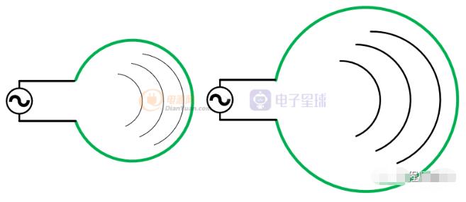
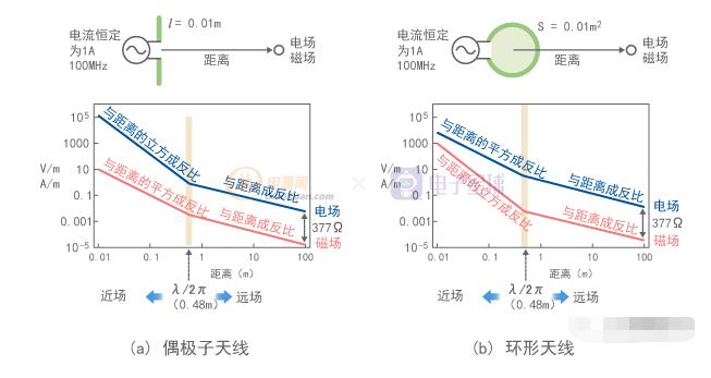
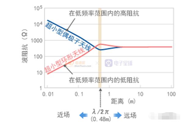
The reflection loss R uses impedance mismatching to reflect noise and suppress interference, which is closely related to impedance. Do you remember 377Ω from earlier? It will be used here in a moment.

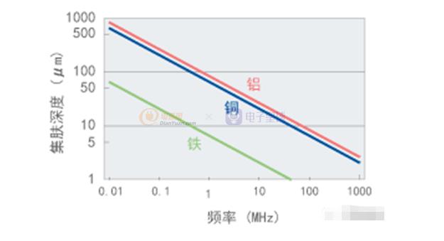
The attenuation loss utilizes the high-frequency skin effect to attenuate the electromagnetic wave, which is related to the shielding material and frequency.

In the previous section, it was mentioned that the wave impedance in the far-field is 377Ω, while shielding materials such as copper have very low impedance due to their high conductivity. 

At 10MHz, the intrinsic impedance of copper is only about 1mΩ, a difference of 300,000 times from the far-field wave impedance. This results in significant reflection, which can achieve an attenuation of 100dB based on reflection coefficient alone.

Using materials with higher conductivity results in greater reflection loss and better shielding effectiveness.

As shown in the figure below, thicker materials result in greater attenuation loss and better shielding effectiveness.

Skin depth is a parameter used to evaluate the strength of skin effect. For materials of the same size, materials with smaller skin depths have stronger interference attenuation and better interference suppression.

The following figure is the key point of this section!

Although the conductivity of iron is lower than that of copper, its magnetic permeability is higher.

From the figure below, it can be seen that at the same frequency, iron has a smaller skin depth than copper. This is because of iron’s higher magnetic permeability, resulting in greater attenuation loss and better interference suppression caused by attenuation loss.

The figure above also shows that the higher the frequency, the smaller the skin depth. Therefore, even very thin metallic materials can achieve good shielding effectiveness at high frequencies.

However!

If the frequency is very low, the skin depth is very large, and thick shielding materials are needed to suppress low-frequency interference. In this case, materials with high magnetic permeability such as iron are better for shielding.

For shielding electric fields from high-frequency interference, thinner materials should be chosen.

For shielding magnetic fields from low-frequency interference, thicker materials should be used. This is how it works.

If you think it’s helpful, welcome to share to your SNS network.

We're ready to help you grow profit with Bamboo charging products in the coming months, don't hesitate to contact us Today!